


Next: Experiment
Up: CE Amp Small Signal
Previous: CE Amp Small Signal
In this chapter, we will only consider operation at frequencies
large enough
where coupling capacitors C1 and C2 can be approximated
to be short-circuits. Furthermore, we will not consider frequencies which
so high that the intrinsic capacitances of the BJT itself
affect circuit performance. These capacitances will be treated in
another lab. Thus we will only be considering circuit performance for these
midband frequences which for BJT circuits typically range from 10kHz to
1MHz.
Having defined our region of frequency operation, let's get back to
amplifiers.
As mentioned above the CE configuration is useful for amplifying
small signal voltages. To understand this refer to Fig. 2.4 and
the following discussion. Recall that a small change in base
current leads to large change in collector current.
Now, this small change in base current can be achieved
by applying a small AC voltage to the base, which in turn will
give rise to a large change in collector current so that
 .It follows that when a relatively large resistor RC is placed
between the power supply VCC and the collector,
the voltage variation across RC and thus the voltage
variation at the collector, due to the large
change in collector current, will also be large.
Thus, a small change in base voltage can lead to a
large change in collector voltage. If we consider the input signal
to be the change in base voltage, and the output signal
to be the change in collector voltage, then the voltage amplification
or gain will be
.It follows that when a relatively large resistor RC is placed
between the power supply VCC and the collector,
the voltage variation across RC and thus the voltage
variation at the collector, due to the large
change in collector current, will also be large.
Thus, a small change in base voltage can lead to a
large change in collector voltage. If we consider the input signal
to be the change in base voltage, and the output signal
to be the change in collector voltage, then the voltage amplification
or gain will be 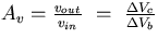 .By choosing the appropriate resistor values, we can design a simple
CE amplifier with the voltage gain we want.
To understand this, consider the following example.
Recall, the voltage gain is
.The general procedure will be to find Vc and Vb from
simple applications of Kirchoff's laws, and then find the
small or incremental changes in these voltages due to an applied
signal at the base.
.By choosing the appropriate resistor values, we can design a simple
CE amplifier with the voltage gain we want.
To understand this, consider the following example.
Recall, the voltage gain is
.The general procedure will be to find Vc and Vb from
simple applications of Kirchoff's laws, and then find the
small or incremental changes in these voltages due to an applied
signal at the base.
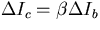
Using KVL directly on the base emitter loop, and recalling that
for most BJT's  , and thus substituting Ie for Ic, gives
If we make an incremental change in Vb by applying a small
signal to the base we obtain:
|  |
(28) |
At this point we could continue our analysis in detail to determine
 . However, it is useful to use our knowledge
of diodes and BJT's to get some insight. Recall, the relationship
between Ic and Vbe is exponential. In other words,
a small change in Vbe leads to a large change in Ic.
Furthermore, once a silicon diode turns on, its voltage drop
will not change much from its DC value of
. However, it is useful to use our knowledge
of diodes and BJT's to get some insight. Recall, the relationship
between Ic and Vbe is exponential. In other words,
a small change in Vbe leads to a large change in Ic.
Furthermore, once a silicon diode turns on, its voltage drop
will not change much from its DC value of  .
Thus is almost always very small. Therefore, a zero order approximation
can often be made to neglect
compared with
.
Thus is almost always very small. Therefore, a zero order approximation
can often be made to neglect
compared with  to yield:
| 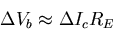 |
(29) |
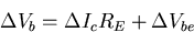
Now let's look at the collector voltage VC.
From KVL we have
Since VCC represents a DC power supply  , therefore
making an incremental change in Vc leads to the following relationship:
, therefore
making an incremental change in Vc leads to the following relationship:
| 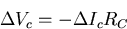 |
(31) |
Taking the ratio  for the voltage gain yields:
| 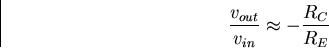 |
(32) |
Equation 2.18
shows
that the approximate voltage gain of the CE amp
is simply the ratio of the collector resistor to the emitter resistor.
It's amazing how far you can get with this simple result.
Next: Experiment
Up: CE Amp Small Signal
Previous: CE Amp Small Signal
Neil Goldsman
10/23/1998