For simple CE amplifiers,
we have to first establish a DC bias condition which means that
we have to choose bias resistors R1 and R2
that give us appropriate values for VC,
VB and VE.
The DC bias point is usually established
to allow for a large variation or swing in vout.
To provide this large swing in vout, a bias network is chosen so that
![]() . In addition, VB and VE
are chosen to be relatively small to make sure that VC > VB
and the BJT does not enter the saturation region.
(Saturation occurs when both the base-emitter and the base-collector
junction are forward biased.)
. In addition, VB and VE
are chosen to be relatively small to make sure that VC > VB
and the BJT does not enter the saturation region.
(Saturation occurs when both the base-emitter and the base-collector
junction are forward biased.)
If the values of R1,R2,RE,RC and VCC are already known, (which is the situation for analyzing existing circuits) the DC bias conditions can be determined by first replacing the voltage divider with its Thevenin equivalent, and then by directly applying loop equations to the circuit while vin=0. To see this consider the circuit in Fig. 2.5.
Using KVL on the base emitter loop, we obtain
| VBB = IBRB+IE RE + VBE | (22) |
The B-E loop
gives one equation and three unknowns.
We can easily reduce the number of unknowns by making the
very good approximations ![]() , and VBE=0.7V.
Using these approximations and recalling that
, and VBE=0.7V.
Using these approximations and recalling that ![]() ,we can obtain the following equation for IC in terms
of known parameters.
,we can obtain the following equation for IC in terms
of known parameters.
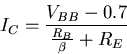 |
(23) |
| VC=VCC-ICRC | (24) |
| VE=IERE | (25) |
| VB=VE+0.7 | (26) |